Hubei DUVTek Co., Ltd. has accumulated achievements in AlN epitaxy technology for many years, and has launched high-quality AlN / AlGaN single-layer and multi-layer full structure epitaxial wafers based on sapphire or SiC, aiming to help deep ultraviolet related scientific research and industrialization.
Based on planar sapphire (FSS), nano patterned sapphire (NPSs) or SiC
High quality AlN or AlGaN monolayers / multilayers with a thickness of 50-5000 nm were grown on different substrates
Especially good at AlN or high Al content AlGaN based template or full structure epitaxy customization, the best al component ≥ 0.4
All structure semiconductor materials of AlGaN based devices such as UV detector, led and HEMT can be customized and grown
We have been developing AlN / AlGaN based optoelectronic devices for a long time. We have a high-quality epitaxial team and rich experience in customized growth of materials
He is good at epitaxial growth of AlN and AlGaN with Al content higher than 0.4 and n-type doping due to the ten years of high temperature MOCVD epitaxial growth
2 inch, XRC (002 / 102) ≤ & nbsp; 80 / 400 arcsec, thickness uniformity (5%), AFM RMS (< 1nm), thickness adjustable 1 ~ 3um
In situ growth of Al based on high quality AlN templatexGa1-xN template, Al component 0.4 ~ 1 adjustable, n-type doping activation concentration ≥ 3e18 cm-3
Product model | Product category | Product pictures | Crystal quality (002) | Crystal quality (102) | Epitaxial thickness | Surface roughness | Marginal deduction | Specification |
---|---|---|---|---|---|---|---|---|
WAlN-SA400 | Sapphire / AlN epitaxial wafer / template | ≤ 80 arcsec | ≤ 400 arcsec | 2~3 μm | ≤ 1 nm | ≤ 3 mm | ||
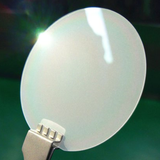
WAlN-NS400 | NPSs / AlN epitaxial wafer / template | ≤ 200 arcsec | ≤ 200 arcsec | ≥ 5 μm | ≤ 1 nm | ≤ 3 mm | ||
WAlN-SC001 | SiC / AlN epitaxial wafer / template | 50~5000 nm | ||||||
WAGN-AN001 | AlGaN epitaxial wafer / template | ≤ 300 arcsec | ≤ 500 arcsec | 1~2 μm | ≤ 2 nm | ≤ 3 mm |
Based on the high-quality AlN and AlGaN material growth technology, the deep violet Technology Division provides customized UV detector, led and HEMT epitaxial growth services
Professional pin, APD, quantum well structure of AlGaN based UV detector research and development, mass production. Years of customized UV detector service experience, serving a number of well-known research institutions and enterprises at home and abroad, with a standard delivery period of one month, providing batch chip OEM service
The upstream epitaxial wafer resources of UVC led for scientific research purposes support scientific research institutions to use commercial UVC LED epitaxial wafers in the frontier exploration and research of nano / micro led. 2 inch, wavelength 270 ~ 280 nm, 3030 chip 120 mA, 8 ~ 12 MW, voltage measurement 10V
Highly customized HEMT epitaxial R & D, pilot service provider, customized growth according to customer structure. Typical square resistance 275 Ω / □, two-dimensional electron gas 1.2e13 cm-3The migration rate was 1900 cm2/Vs
The full structure materials grown by our epitaxial team have entered all aspects of civil life, industrial application and space exploration after being made into devices